Conventional wisdom in semiconductor manufacturing has long held that bigger chips mean worse yields. Yet at Cerebras, we’ve successfully built and commercialized a chip 50x larger than the largest computer chips – and achieved comparable yields. This seeming paradox is one of our most frequently asked questions: how do we achieve a usable yield with a wafer-scale processor?
The answer lies in rethinking the relationship between chip size and fault tolerance. This article will provide a detailed, apples-to-apples comparison of manufacturing yields between the Cerebras Wafer Scale Engine and an H100-sized chip, both manufactured at 5nm. By examining the interplay between defect rates, core size, and fault tolerance, we’ll show how we achieve wafer scale integration with equal or better yields vs. reticle limited GPUs.
What determines yield
Like any manufacturing process, computer chips are prone to defects. Larger chips are more likely to encounter defects, thus as chips grow in size, yields fall exponentially with increasing die area. Even though larger chips generally run faster, early microprocessors were built to a modest size to maintain acceptable manufacturing yields and profit margins. In the early 2000s, this started to change. As transistor budgets grew to over 100 million, it became the norm to build processors with multiple independent cores per chip. Since all the cores were identical and independent, chip designers built-in core-level fault tolerance so that if one core suffered a defect, the remaining cores could still operate. For example in 2006 Intel released the Intel Core Duo – a chip with two CPU cores. If one core was faulty, it was disabled and the product was sold as an Intel Core Solo. Nvidia, AMD, and others all embraced this core-level redundancy in the coming years.
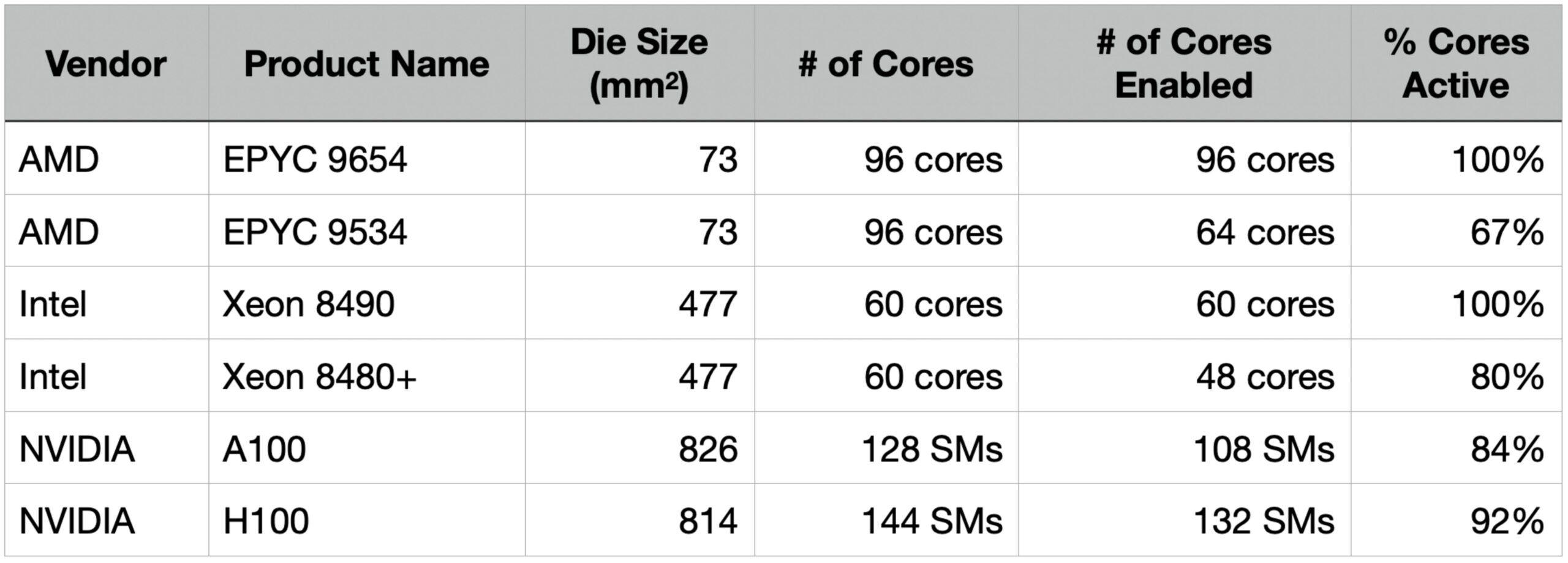
Today, fault tolerance is widely used by high performance processors and it’s perfectly normal to sell chips with some cores disabled. AMD and Intel CPUs generally ship a flagship version with all cores enabled and a lower end version with a portion of cores disabled. Nvidia’s data center GPUs are substantially larger than CPU dies and as a result even its flagship models have some portion of cores disabled.
Take the Nvidia H100 – a massive GPU weighing in at 814mm2. Traditionally this chip would be very difficult to yield economically. But since its cores (SMs) are fault tolerant, a manufacturing defect does not knock out the entire product. The chip physically has 144 SMs but the commercialized product only has 132 SMs active. This means the chip could suffer numerous defects across 12 SMs and still be sold as a flagship part.
Defect tolerance is the key to yield
Traditionally, chip size directly dictated chip yields. In the modern era, yield is a function of both chip size and defect tolerance. 800mm2 chips were once thought infeasible to commercialize due to yield, but by using defect tolerant design, they are now mainstream products.
The degree of defect tolerance can be measured by the amount of chip area that is lost when a defect occurs. For multi-core chips, this means the smaller the core, the greater the defect tolerance. If individual cores are small enough, it may be possible to build a very large chip.
Wafer Scale Engine Cores
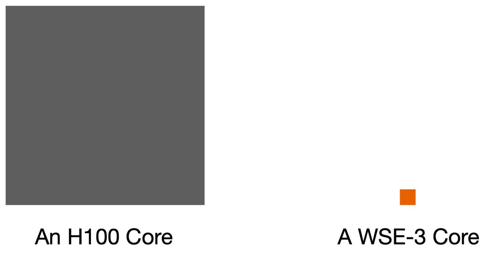
At Cerebras, before committing to build a wafer-scale chip, we first designed a very small core. Each AI core in the Wafer Scale Engine 3 is approximately 0.05mm2 or about 1% the size of an H100 SM core. Both core designs are fault tolerant. This means a defect in a WSE core would disable 0.05mm2 of silicon while the same defect in an H100 disables ~6mm2. To a first order of approximation, the wafer scale engine is ~100x more fault tolerant than a GPU when considering the silicon area affected by each defect.
The Routing Architecture
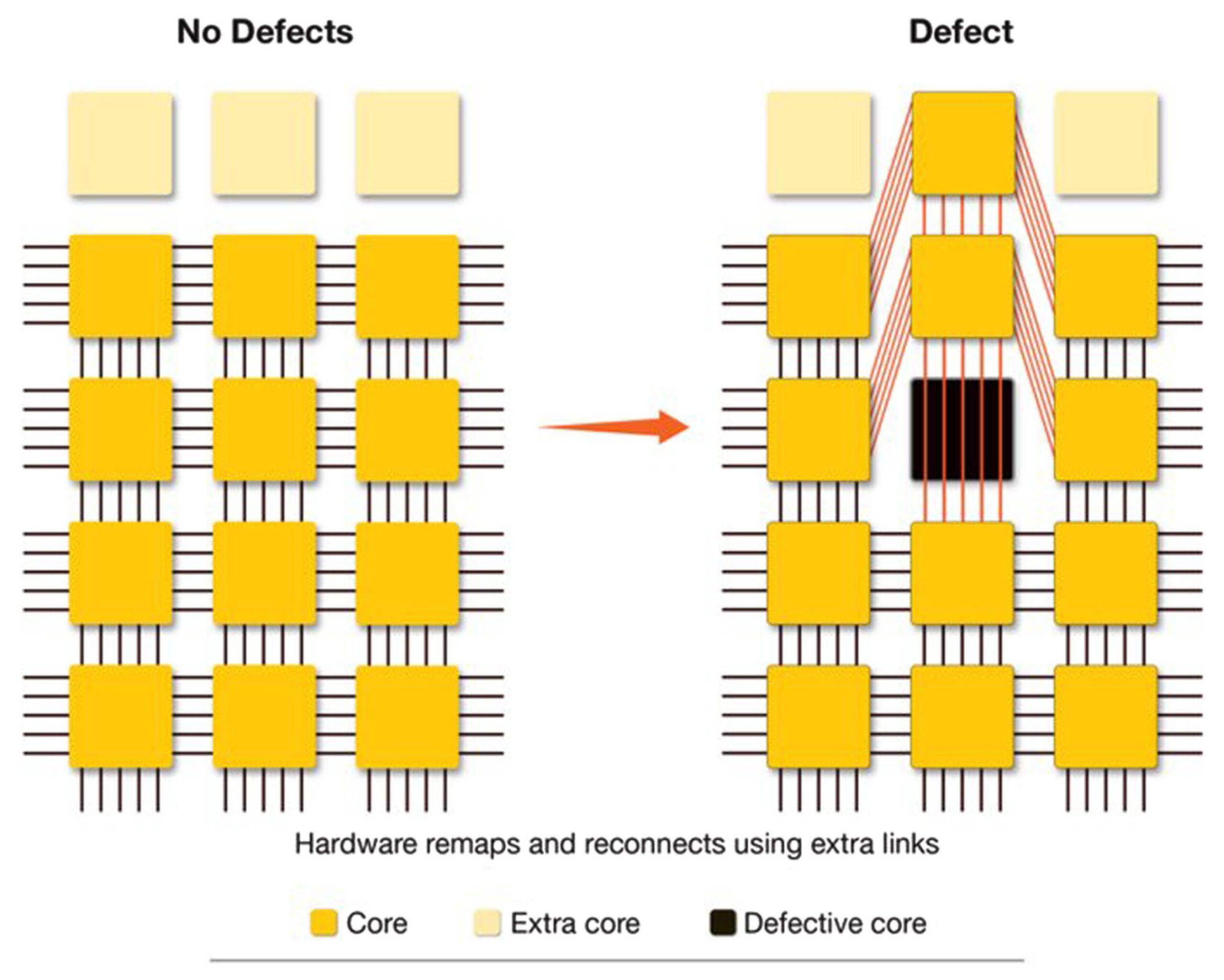
But small cores alone aren’t enough. We developed a sophisticated routing architecture that allows us to dynamically reconfigure connections between cores. When a defect is detected, the system can automatically route around it using redundant communication pathways, preserving the chip’s overall computational capabilities by leveraging nearby cores.
This routing system works in concert with a small reserve of spare cores that can be used to replace defective units. Unlike previous approaches that required massive redundancy overhead, our architecture achieves high yield with minimal spare capacity through intelligent routing.
A wafer scale walkthrough
Defect tolerance at a chip level is fairly clear. Let’s now compare how a traditional GPU and a wafer-scale chip would yield using TSMC 5nm’s 300mm wafer:
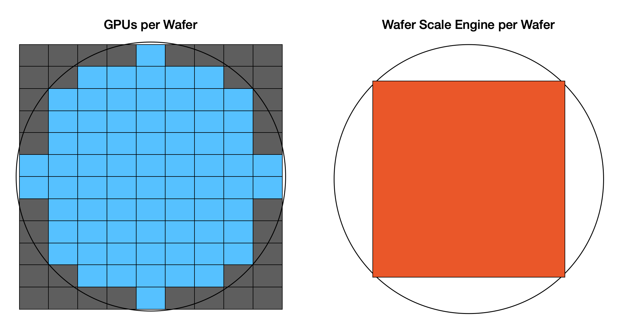
On the left is a H100-like GPU: it is 814mm2, it has 144 fault tolerant cores, and a single 300mm wafer yields 72 full die chips. On the right we have the Cerebras Wafer Scale Engine 3. It’s one giant square measuring 46,225mm2. It has 970,000 fault tolerant cores. One wafer yields one chip.
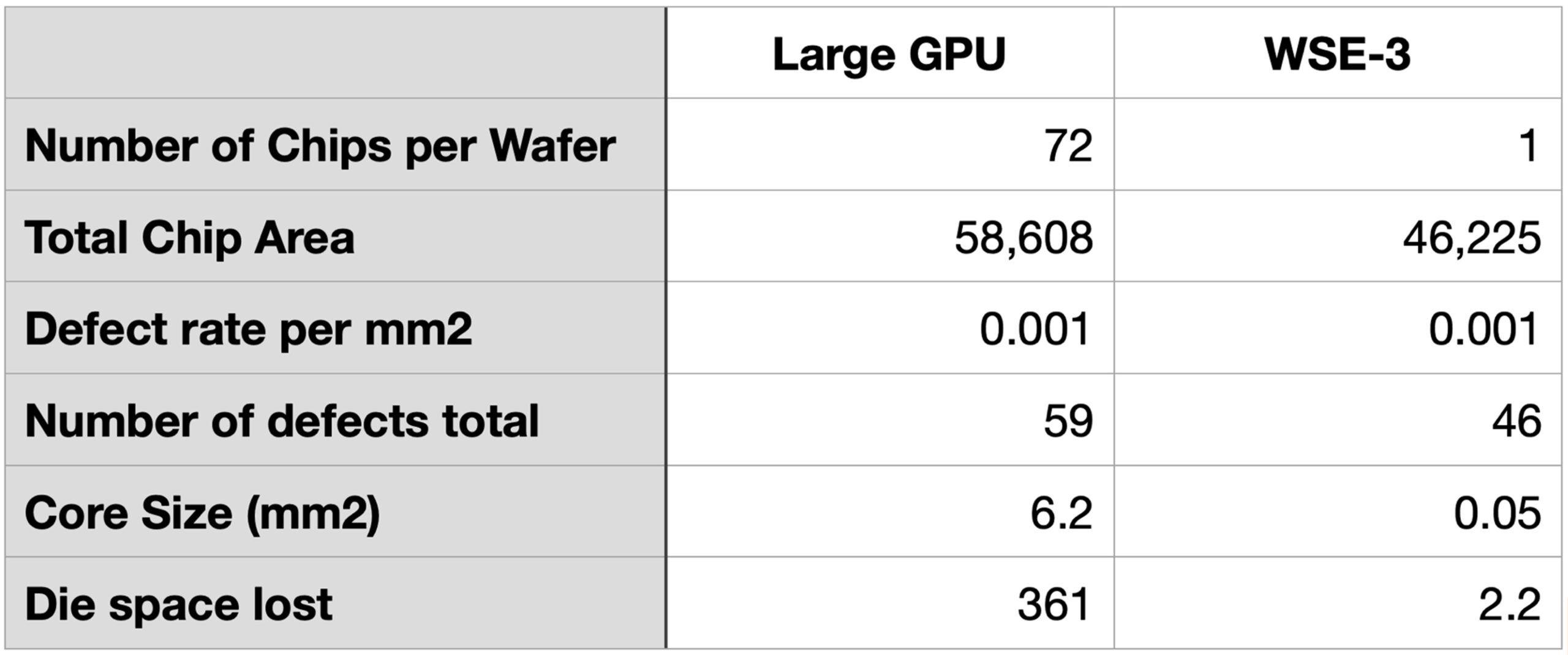
At the current TSMC 5nm node, TSMC’s process reportedly has ~0.001 defect per mm2. 72 GPU dies have total die area of 58,608mm2. Applying this defect density, this area would see a total of 59 defects. For simplicity, let’s assume each defect lands on a separate core. At 6.2mm2 per core, this means 361mm2 of die space would be lost of defects.
On the Cerebras side, the effective die size is a bit smaller at 46,225mm2. Applying the same defect rate, the WSE-3 would see 46 defects. Each core is 0.05mm2. This means 2.2mm2 in total would be lost to defects.
Measuring the total area lost, the GPU in this case loses 164x more silicon area than the Wafer Scale Engine on an apple-to-apples basis on the same manufacturing node and defect rate.
The above makes a high-level point but simplifies a few details. First, not all areas of the chip are taken by the compute cores. Caches, memory controllers, and on-chip fabric take up a substantial amount of die size, perhaps up to 50%. However, these components can be designed to be fault tolerant in their own way. An H100 SM is likely smaller than 6.2mm2 due to these components, though not by an order of magnitude. Second, a cluster of defects could overwhelm fault tolerant areas and disable the whole chip. In practice, even fault tolerant chips will not yield close to 100%. These caveats aside, the general rule that smaller cores make for greater fault tolerance still holds.
Putting Cerebras in the Table
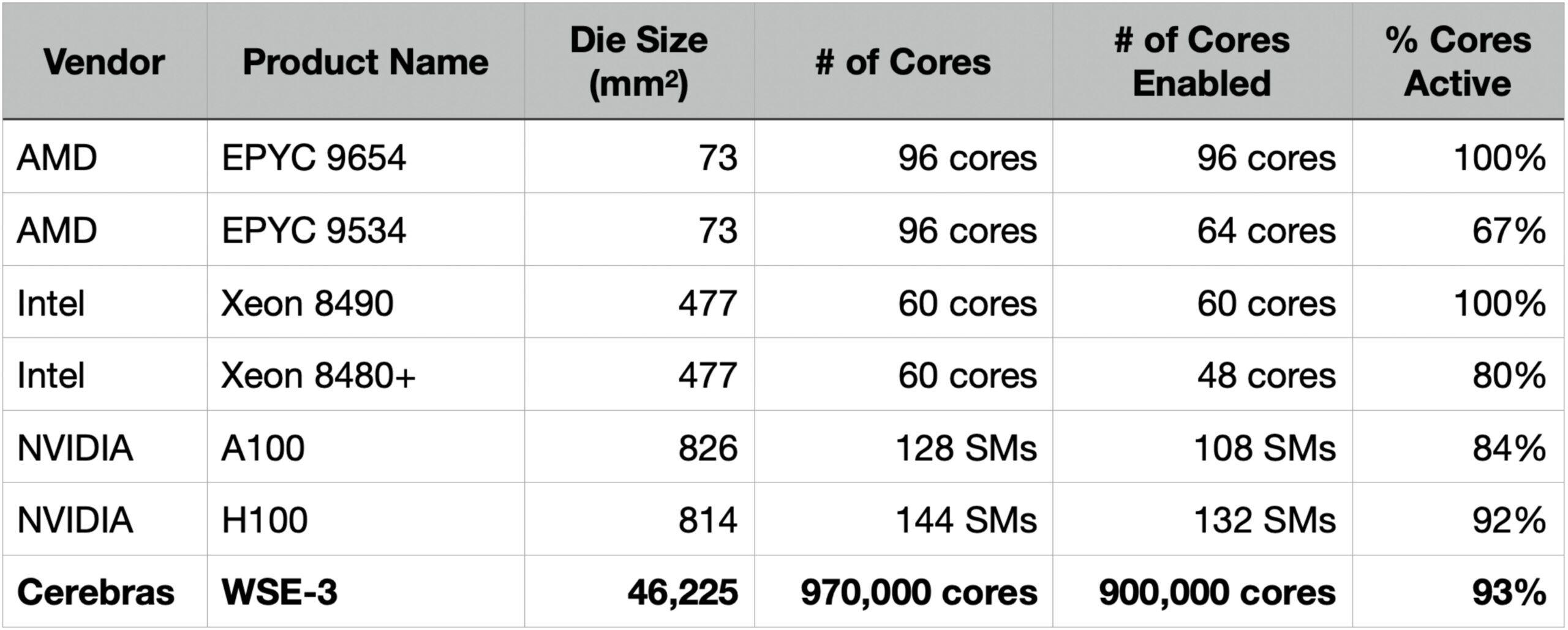
Let’s revisit the first table, now with the Cerebras Wafer Scale Engine added. Like Nvidia’s data center GPUs, the WSE-3 is designed to be fault-tolerant and disables a portion of its cores to manage yield. Because our cores are so tiny, the number of cores is so much larger – 970,000 physical cores with 900,000 active on our current shipping product. This provides tremendous, fine grained, defect tolerance. Despite having built the world’s largest chip, we enable 93% of our silicon area, which is higher than the leading GPU today.
To summarize, Cerebras resolved the wafer scale manufacturing challenge by designing a small fault-tolerant core in combination with a fault tolerant on-chip fabric. While total chip area increased by ~50x compared to conventional GPUs, we reduced individual core size by ~100x. As a result, defects are far less damaging to the WSE than conventional multi-core processors. The third generation WSE engine achieves 93% silicon utilization – the highest among leading AI accelerators – demonstrating that wafer-scale computing is not just possible, but commercially viable at scale.